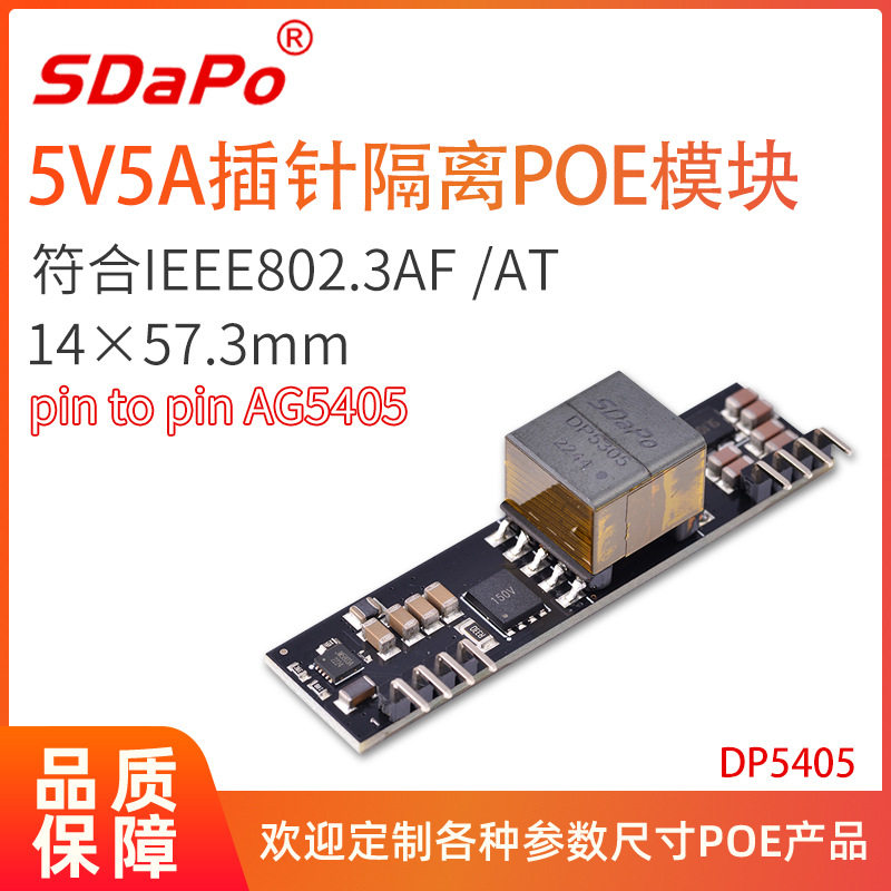
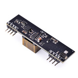
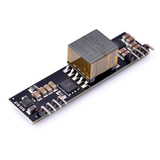
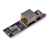
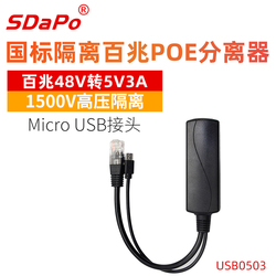
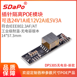
DP5405 Docking Ag5405 Синхронизация выпрямитель высокая эффективность, способная 92% патч -модуль Sdapo dapo
Вес товара: ~0.7 кг. Указан усредненный вес, который может отличаться от фактического. Не включен в цену, оплачивается при получении.
Описание товара


- Информация о товаре
- Фотографии
| Цвет: | 5V4-5A Gigabit Module POE |
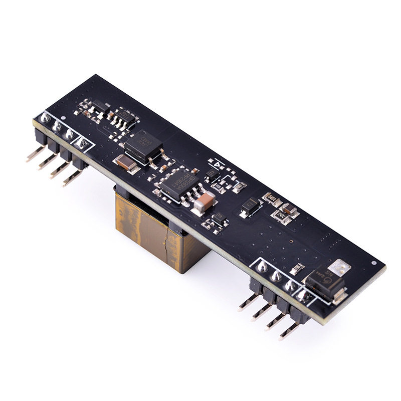
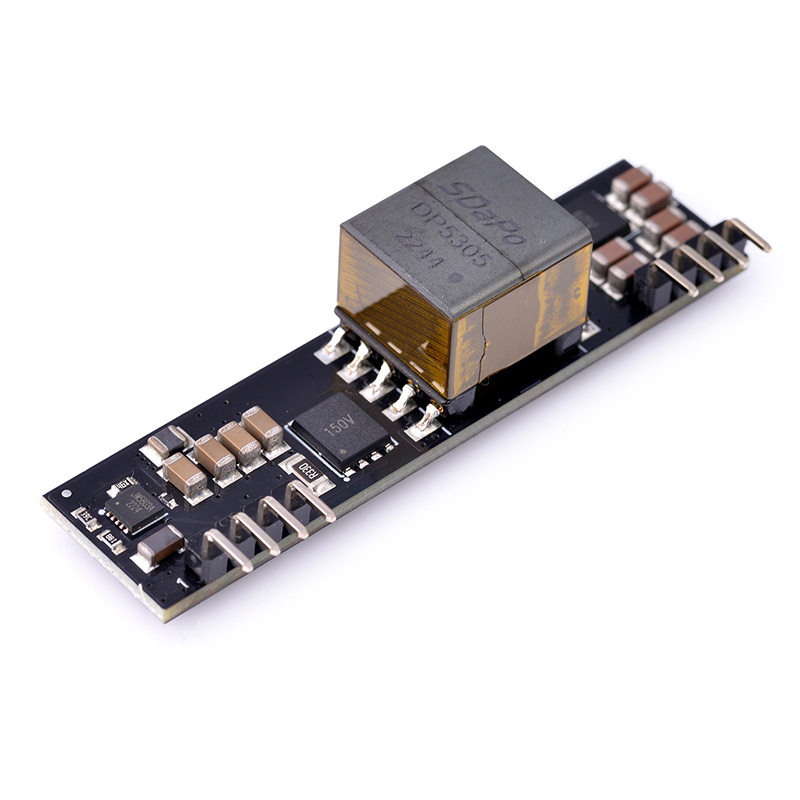

DESCRIPTION
5V5A,25WPD(Powered Device)IntegratedModule(IsolationType)
FEATURES
Fully supports IEEE802.3af/at
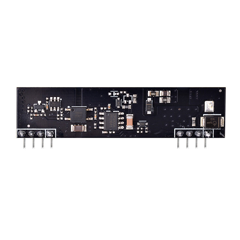
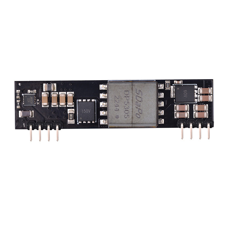
Небольшой встроенный (SIL) размер упаковки 57,3 мм (L) x 14 мм (ч)
lnput Voltage Range 44V to 57V
Support PoE applications in both of Fast / Gigabit Ethernet environments.
Short Circuit Protection
Over-temperature Protection
Programmable Classification (Default:Class 4)
High Efficiency
Isolation level 1.5KVrms.
Easy Installation and Low Cost (Isolation Type, Minimum External Devices required)
Low Output Ripple and Noise
Adjustable Output Voltage
1500Vrms Isolation (Input-Output)
Pin Description
1 | VIN+
| POE Direct Input +. Этот контакт подключается к положительному (+) выходу. of the POE input bridge rectifiers. |
2 | VIN-
| POE Direct Input -. Этот контакт подключается к отрицательному (-) выходу. of the POE input bridge rectifiers. |
3 | AT Detect Output | AT Detect Output.Этот вывод указывает, подает ли PSE IEEE802.3at питание наDP5400; |
4 | NC | Internal Connection.Do not connect to this pin. |
5 | -VDC
| Negative DC Output.Этот контакт обеспечивает отрицательный регулируемый output from the Ag5400 and is internally connected to pin8. |
6 | +VDC
| Positive DC Output.Этот контакт обеспечивает положительный регулируемый output from theDP5400. |
7 | ADJ
| Output Adjust.Выходное напряжение можно регулировать в зависимости от его номинальное значение, подключив внешний резистор от этого контакта либо к выводу +VDC, либо к выводу -VDC. |
8 | -VDC
| Negative DC Output.Этот контакт обеспечивает отрицательный регулируемый output from the Ag5400 and is internally connected to pin5. |
Figure4: Output Adjustment
Reducing the output voltage, connect R between ADJ and +VDC | |||
Value of R | DP5405 output | DP5412 Output | DP5424 Output |
Open Circuit | 5.00V | 12.07V | 23.93V |
0 Ohms | 4.48V | 10.0V | 19.85V |
100K | 4.76V | 11.15V | 21.85V |
470k | 4.92V | 11.76V | 23.23V |
| |||
Increasing the output voltage, connect R between ADJ and -VDC | |||
Value of R | DP5405 output | DP5412 output | DP5424 Output |
Open Circuit | 5.00V | 12.07V | 23.93V |
0 Ohms | 5.66V | 12.75V | 24.6V |
100K | 5.27V | 12.34V | 24.2V |
470k | 5.08V | 12.16V | 24.01V |
Table 3: Output Adjustment Resistor (R) Value
Electrical Characteristics
3.1Absolute Maximum Ratings
| Parameter | Symbol | Min | Max | Units |
1 | DC Supply Voltage | VCC | -0.3 | 60 | V |
2 | DC Supply Voltage Surge for 1ms | VSURGE | -0.6 | 80 | V |
3 | Storage Temperature | TS | -40 | +100 | МрачныйC |
3.2Recommended Operating Conditions
| Parameter | Min | Typ | Max | Units |
1 | Input Supply Voltage | 36 | 52 | 57 | V |
2 | Under Voltage Lockout | 30 |
| 36 | V |
3 | Input Curren |
| 600 | 660 | mA |
4 | Operating Temperature | -40 | 25 | 85 | ℃ |
5 | Output capacitance |
| 470 | 1000 | uF |
6 | IEEE 802.3at | Class 4 | |||
3.3DC Electrical Characteristics
| DC Characteristic | Sym | Min | Typ1 | Max | Units |
1 | Nominal Output Voltage | +VDC | 4.9 | 5 | 5.1 | V |
2 | Minimum Load | ILOAD | 100 |
|
| mA |
3 | Output Current (VIN = 52V) | Iout |
| 4 | 5 | A |
4 | Line Regulation |
|
| 0.05 |
| % |
5 | Load Regulation - Min to Max (VIN = 52V) |
|
| 0.1 |
| % |
6 | Output Ripple and Noise5@ Max load |
|
| 140 |
| mVp-p |
7 | Peak Efficiency |
|
| 91 |
| % |
8 | Short-Circuit Duration2 |
|
|
| ∞ | sec |
9 | Isolation Voltage (I/O) - Impulse Test | VISO |
|
| 1500 | VPK |
Note 1: Typical figures are at 25°C with a nominal 52V supply and are for design aid only. Not Guaranteed
Note 2: >250mohm short due to thermal limitation.


